Choose timezone
Your profile timezone:
Reducing the dimensionality of an electronic device makes life easier for theorists, but harder for experimentalists who must design low-dimensional materials in a three-dimensional world. The rise of isolated two-dimensional (2D) materials such as graphene was a breakthrough in this respect and led to a very active field of research ranging from crystal growth to theoretical modelling. New compounds, ranging from insulators to superconductors, are announced on a weekly basis, with intriguing properties distinct from their 3D counterparts.
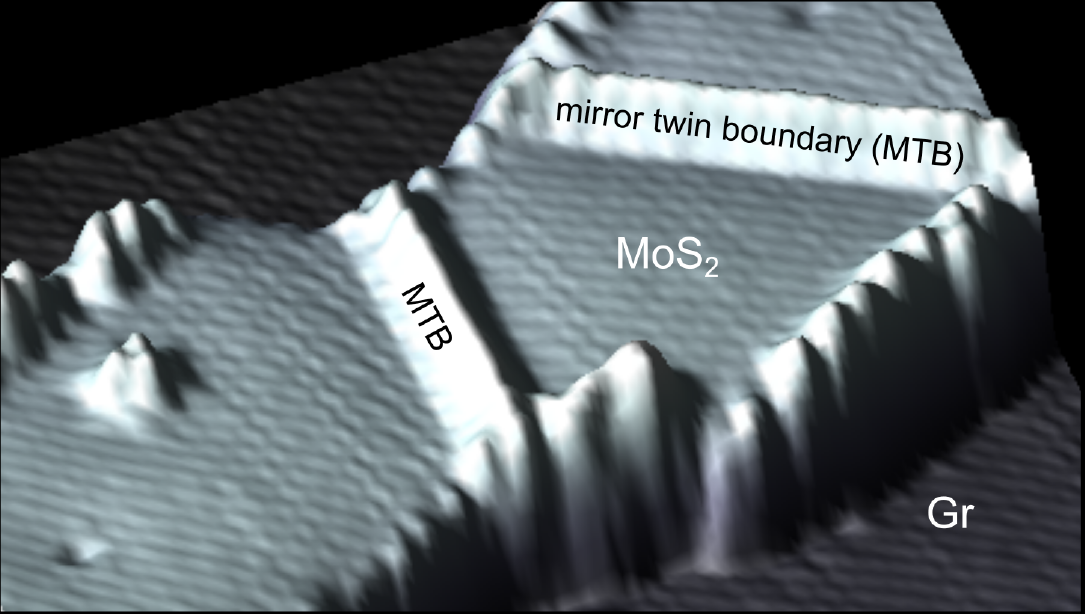
In my talk I will give an overview on 2D materials and show how surface science methods such as scanning tunnelling microscopy represent the ideal tools to access the physical properties of these all-surface materials. Furthermore, I will focus on the possibility to reduce dimensionality even further by constructing one-dimensional (1D) conductors in a 2D semiconductor (MoS2) using mirror twin boundaries, a highly symmetric line defect. Finally, I will show our recent attempt to fully localize electrons in real space while dynamically control their spin degree of freedom on the atomic scale.
invited by AG Busse